3D Chip Stacking & Chiplets for Edge AI: The Semiconductor Shift Powering 2026 and Beyond
5 min readEr.Muruganantham
The semiconductor industry is approaching a physical limit that software alone cannot solve.
Transistor scaling is slowing, power density is rising, and AI workloads are exploding — especially at the edge, where power, latency, and thermal budgets are tightly constrained. In response, the industry’s focus has shifted from smaller transistors to smarter packaging.
At the center of this shift are 3D chip stacking and chiplet-based architectures.
By 2026, these technologies are expected to deliver 2× gains in density and performance, fundamentally reshaping AI accelerators, edge devices, and even early quantum systems.
Why Traditional Chip Scaling Is No Longer Enough
For decades, performance gains came from shrinking transistors. That era is ending due to:
- rising leakage currents
- thermal density limits
- exponential fabrication costs
- diminishing frequency gains
AI accelerators, NPUs, and edge inference chips demand:
- massive memory bandwidth
- low latency
- strict power envelopes
Flat, monolithic chips can no longer meet these demands efficiently.
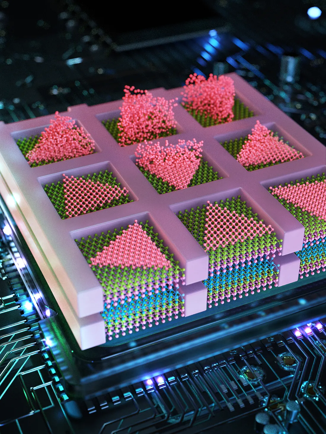
What Is 3D Chip Stacking?
3D chip stacking places multiple silicon dies on top of each other instead of side by side.
Key characteristics:
- vertical interconnects (TSVs or hybrid bonding)
- dramatically shorter signal paths
- higher bandwidth at lower power
- better silicon utilization
Instead of data traveling across a PCB, it moves micrometers vertically.
This is transformational for AI.
Chiplets: Modular Silicon for the AI Era
A chiplet is a small, specialized die that performs a specific function:
- compute
- memory
- I/O
- power management
Rather than building one massive chip, manufacturers:
- design multiple chiplets
- fabricate them on optimal process nodes
- assemble them into one package
This approach improves:
- yield
- cost efficiency
- scalability
- design flexibility
Chiplets + 3D stacking = modular vertical systems.
HBM: The Memory Backbone of AI Accelerators
High Bandwidth Memory (HBM) is the most visible success of 3D stacking today.
HBM works by:
- stacking DRAM dies vertically
- connecting them with TSVs
- placing them directly next to or on top of logic dies
Benefits:
- orders of magnitude higher bandwidth
- far lower energy per bit
- reduced memory bottlenecks
Modern AI accelerators rely on HBM not as an optimization — but as a necessity.
Why This Matters for Edge AI (Not Just Data Centers)
Edge AI devices operate under constraints:
- limited power budgets
- minimal cooling
- real-time response requirements
3D-stacked chiplets enable:
- more compute per watt
- localized memory access
- smaller form factors
This allows advanced inference to run:
- on AI PCs
- in vehicles
- on industrial sensors
- in smart infrastructure
Without cloud round-trips.
The Rise of NPUs in AI PCs
Industry projections indicate that by 2026, approximately 57% of AI PCs will ship with dedicated NPUs.
Why NPUs matter:
- offload AI tasks from CPUs/GPUs
- operate at much lower power
- handle always-on inference workloads
Chiplet-based NPUs make this feasible at scale by:
- reusing proven IP blocks
- stacking memory tightly with compute
- reducing idle power draw
This is not speculative — it is already appearing in next-generation client silicon.
Wide-Bandgap Materials: GaN and SiC Enter the Picture
While logic chips handle computation, power electronics determine efficiency.
Wide-bandgap semiconductors like Gallium Nitride (GaN) and Silicon Carbide (SiC) offer:
- higher breakdown voltage
- faster switching
- lower conduction losses
- better thermal performance
In EVs and data centers, these materials can reduce power losses by up to 40%.
As AI hardware scales, energy efficiency is becoming as important as compute density.
Python’s Role in 3D IC and Chiplet Design
Hardware design is no longer isolated from software.
Python has become a dominant tool in:
- device simulation
- material modeling
- visualization
- early-stage architecture exploration
Frameworks like SemiX (and similar Python-based research tools) allow engineers to:
- simulate diode and transistor behavior
- model thermal and electrical interactions
- visualize GaN/SiC material characteristics
- explore 3D interconnect effects
This lowers the barrier for researchers and accelerates experimentation.
Why Researchers Are Moving to Python-Based Simulation
Python offers:
- rapid prototyping
- strong scientific libraries
- visualization ecosystems
- integration with ML models
In 3D IC research, Python is often used to:
- validate device models
- predict performance bottlenecks
- analyze thermal stress
- explore design trade-offs before fabrication
This trend is especially strong in academic and early-industry research.

Quantum and Advanced Accelerators: Early Beneficiaries
While quantum computing is still emerging, 3D integration is already critical:
- dense qubit placement
- reduced signal latency
- improved cryogenic wiring efficiency
The same stacking techniques used for AI accelerators are being adapted — carefully — for quantum research.
This cross-pollination accelerates innovation in both fields.
Key Drivers Behind the 2026 Shift
Several forces are converging:
- AI workloads growing faster than transistor scaling
- edge inference becoming mainstream
- energy costs rising globally
- sustainability requirements tightening
- manufacturing economics favoring modularity
3D chip stacking and chiplets are not optional upgrades — they are structural solutions.
Challenges That Still Remain
Despite the promise, there are real hurdles:
- thermal management in stacked dies
- complex packaging yields
- design and verification complexity
- interconnect standards and tooling
These challenges are why software simulation, modeling, and tooling are critical today.
Conclusion
The future of AI hardware will not be defined by smaller transistors alone.
It will be shaped by:
- 3D chip stacking
- chiplet-based architectures
- HBM integration
- wide-bandgap materials
- software-driven design tools
For edge AI, this shift enables:
- higher performance per watt
- compact, efficient devices
- real-time intelligence outside the cloud
The semiconductor industry is not slowing down — it is restructuring itself vertically.
References
- Advanced Packaging and 3D IC Trends: https://www.semi.org
- High Bandwidth Memory (HBM) Overview: https://www.jedec.org
- Chiplet Architectures and Design Economics: https://www.anandtech.com
- Wide-Bandgap Semiconductors (GaN, SiC): https://www.powerelectronics.com
- Python in Semiconductor Research: https://scipy.org
More in technology


Cubed
Write about the technologies shaping the future.
For developers, founders, and curious minds exploring AI, crypto, Web3, and emerging tech—signal over noise.
One free account across In Plain English, Stackademic, Venture, and Cubed.
How it works- AI, crypto & Web3
- Software & emerging technologies
- Analysis & practical resources
- Thoughtful voices, not hype
Sign in
Google or GitHub
Complete profile
Takes a few minutes
Get approved & publish
Start sharing
Why write for Cubed?
The future deserves thoughtful voices, not just louder headlines.
Comments
Loading comments…